Multilayer PCBs
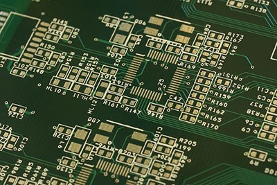
Multilayer PCBs are getting attention in the electronics industry, and their demand is rising. The craze is because designers are now looking for more powerful, faster, and yet smaller circuit boards. Unfortunately, double and single-sided boards cannot open up possibilities like multilayer PCBs.
Engineers are lucky that there is a circuit board available that has enough space to accommodate their sophisticated designs. Multilayer PCB is made up of both single and double-sided PCBs. So, you will get higher assembly density and much more! This article explains all the details related to Multilayer PCB; keep on reading.
Among the key subjects on Multilayer PCBs include

- Multilayer PCB:In this section, we introduced multilayer PCBs and their need.
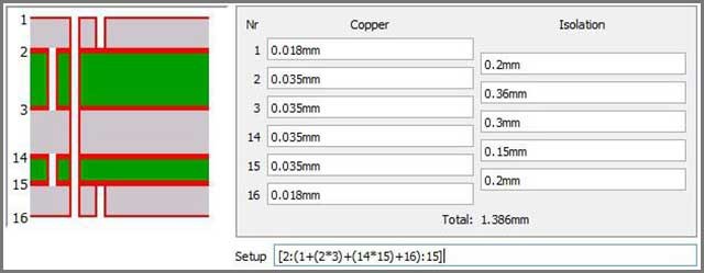
- Designing the Multilayer PCB: This section focuses on multi-layer PCB information about its construction and design rules.
- Complications related to Multilayer PCB: This section focuses on the two complications of this field.
And describes the consequences of adding more layers And how to identify them by looking at the board.
Follow the following steps:
- Shine a light on the board edge to see the copper planes. You will be able to see signal traces more thoroughly.
- Use bright light to examine the inner layers of the multilayer PCB.
- The best area to look for inner layers is where you cannot see paths or lines on the outer layer.
- You can also look around the edge to read the number of layers. Some manufacturers print the total number of segments on the board.

Advantages of Multilayer PCB: This section highlights the benefits of multi-layer PCBs
- Higher assembly density, function, and speed;
- PCB size is getting smaller and smaller;
- Multilayer PCBs are also lighter in weight;
- Design enhancements.
Limitations of Multilayer PCB: This section focuses on the restraints of multi-layer PCBs
- High cost: If you are a budget person, you should take into account the total project cost before selecting a multilayer PCB.
- More Manufacturing Time: If you are time-conscious or have less time for completion of the project, then this is a significant limitation.
- Complex Repair: Multilayer PCB need a more complicated mending procedure when you compare it with other types of PCBs.
Applications of Multilayer PCB: This section mainly introduces its significant applications.
① Data storage
② Signal transmission
③ Computers
④ File servers
⑤ GPS technology
⑥ Industrial controls
⑦ Test equipment
⑧ X-ray equipment
⑨ Cell phone transmission
⑩ Central fire alarm systems
⑪ Cat scan technology
⑫ Cell phone repeaters
⑬ Handheld devices
⑭ Atomic accelerators
⑮Nuclear detection systems
⑯Space probe equipment
⑰Fibre optic receptors
⑱Weather analysis
⑲Heart monitors
⑳Satellite systems
In conclusion
In conclusion, we would say that electronic designs are getting complicated daily. Designers are looking for more wiring areas and need PCBs that are small in size. So, in this case, multilayer PCBs are your solution.
We have added all the necessary information related to multilayer PCBs. This article will help you decide whether to use them over other types. Here at WellPCB, we can manufacture your multilayer PCBs with high quality. All you need to do is to go to our website and place an order.
You will need to fill in some specifications in your PCB while placing the order. After that, our Engineers will check your order, and soon, an instant quote will also appear. Then, your multilayer PCB will be at your doorstep as we also offer quick deliveries.
If you want to know other articles on the website, for example, PCB Silkscreen Manufacturing Services, please click here to view! Customwiringloom.com and WellPCB.com are brother companies. It specializes in the production of precise Board Solar Photoelectric connectors, I/O connectors, industrial Terminal blocks, and cable assemblies for computer & peripheral devices.


